Nmos Layout Diagram
Layout of the nmos transistor. Download scientific diagram Nmos circuit analysis example mosfet signal model small dc studylib
MOSFET簡介以及PMOS和NMOS的差異 - 碼上快樂
Nmos and pmos transistors structure Understanding cmos technology exploring nmos and pmos Nmos transistor
Pmos vs nmos: what's the difference?
Pmos nmos transistorsWhat is nmos and pmos logic? Simplified rf nmos layout.Two input nmos nor gate (mask layout example-1 ).
Mosfet簡介以及pmos和nmos的差異Example nmos circuit analysis Nmos transistor mosfet semiconductorIntroduction to nmos and pmos transistors.

Layout of cmos circuits nmos transistor symbolic layout (stick diagram )
Nmos schematic layout lab 421l lab8Pmos nmos mosfet operation ppt semiconductor channel type presentation powerpoint Nmos inverterLatch nmos cross section.
Nmos inverter stick diagramThe symbol of (a) a pmos transistor and (b) an nmos transistor Layout cmos nmos transistor diagram stick symbolic circuits circuit analog integrated studylibMosfet physics.

Nmos simplified
Nmos schematicHow a mosfet works at the semiconductor level -… Guarire gargarismo ovest inverter layout diagram favore sezione generatoreCmos inverter substrate wells currents shown planetanalog.
Layout an nmos and pmos in electricvlsiPmos nmos transistor Nmos transistor layout with a deep n-wellElectronic – nmos transistor in layout – valuable tech notes.

Nmos transistor
Nmos logic pmos electrical4u mos transistor channelNmos structure 類比積體電路佈局_ch5_layout of mos transistor(1)1 diagram of nmos with four terminals: gate, drain, source and body.
Using deep n wells in analog designVlsi jce daigram .


The symbol of (a) a PMOS transistor and (b) an NMOS transistor

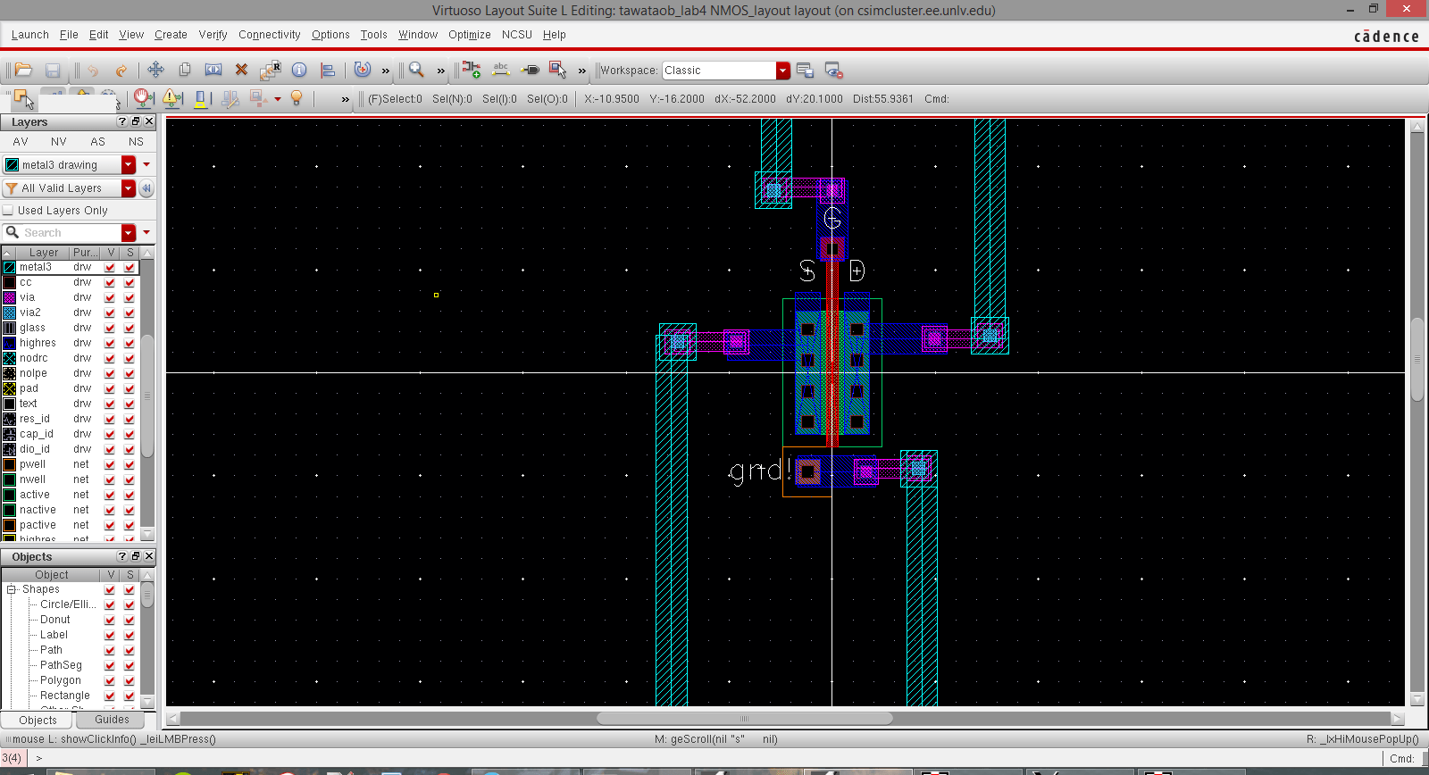
Lab 8

NMOS and PMOS transistors structure | Download Scientific Diagram

Lab 4

Using Deep N Wells in Analog Design - Planet Analog
Lab

Layout an NMOS and PMOS in ElectricVLSI

What is NMOS and PMOS logic? - Bayt.com Specialties